
Master thesis - Optimization of Plasma enhanced chemical vapor deposition (PECVD) Thin Films (m/f/d)
Premstätten, Styria, Austria – ams-OSRAM AG
What we expect
- Process Analysis and Development:
- Understand the role of PECVD in depositing essential dielectric layers, such as SiO₂ and Si₃N₄ for CMOS devices.
- Investigate the impact of PECVD process parameters (e.g., precursor gas ratios, RF power, pressure, substrate temperature) on film stoichiometry.
- Identify correlations between input parameters and key output metrics like film thickness and RI.
- Experimental Design and Execution:
- Develop systematic experiments using Design of Experiments (DoE) techniques.
- Perform thin film deposition runs on state-of-the-art equipment available at ams-OSRAM's fabrication facilities.
- Metrology and Characterization:
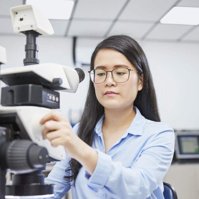
- Characterize deposited thin films using ellipsometry to assess thickness and refractive index and Scanning Electron Microscopy (SEM) with Energy Dispersive X-ray Spectroscopy (EDX) to evaluate stoichiometric composition.
- Evaluate process stability, within-wafer and wafer-to-wafer uniformity.
- Data Analysis and Optimization:
- Analyze experimental data using statistical tools and regression models.
- Propose optimized PECVD recipes that meet stringent CMOS specification targets.
- Derivation of Fit and Response models for process parameter tuning to optimize process capability.
- Reporting and Communication:
- Document all process steps, experimental results, and analysis findings.
- Present progress in regular meetings with supervising engineers and researchers.
- Compile a final thesis report containing conclusions, visualized data, and future recommendations.
Who we are looking for
- Currently enrolled in a Master’s program in Materials Science, Electrical Engineering, Physics, Nanotechnology, Chemical Engineering, or a related field.
- Foundational understanding of:
- Thin film deposition processes, especially CVD.
- Semiconductor device fabrication and CMOS technology basics.
- Basic knowledge of plasma and vacuum physics
- Experience with laboratory work, especially in a semiconductor or cleanroom environment, is advantageous.
- Proficiency in data analysis tools such as Minitab and MATLAB is beneficial.
- Strong analytical mindset, hands-on problem-solving abilities, and attention to detail.
- Good communication skills in English (spoken and written), proactively and independent working style.
We offer competitive salaries and additional benefits based on your performance, experience, and qualifications. Employment is in accordance with the collective agreement for the electrical and electronics industry, employment group E (https://www.feei.at/aktuelles/mindestloehne-und-gehaelter-eei/).
Contact

Marlies Nigitz will be happy to answer any questions you may have.
Phone: +43 3136 500 32853
E-Mail: marlies.nigitz@ams-osram.com
For data protection reasons, we only accept applications submitted through our applicant portal. This allows you to view the status of your application in your profile at any time.
Job details
| Posting date: | 2025/11/11 |
|---|---|
| Experience level: | Student |
| Type of contract: | Bachelor/Master Thesis |
| Employment type: | Part-time |
| Work Model: | On site |
| Business unit: | CMOS Sensors & ASICs |
| Organization: | ams-OSRAM AG |
| Job field: | Administration & Services |
| Job ID: | 21488 |